
Scanning Auger Nanoprobe
Room 105 NPIC
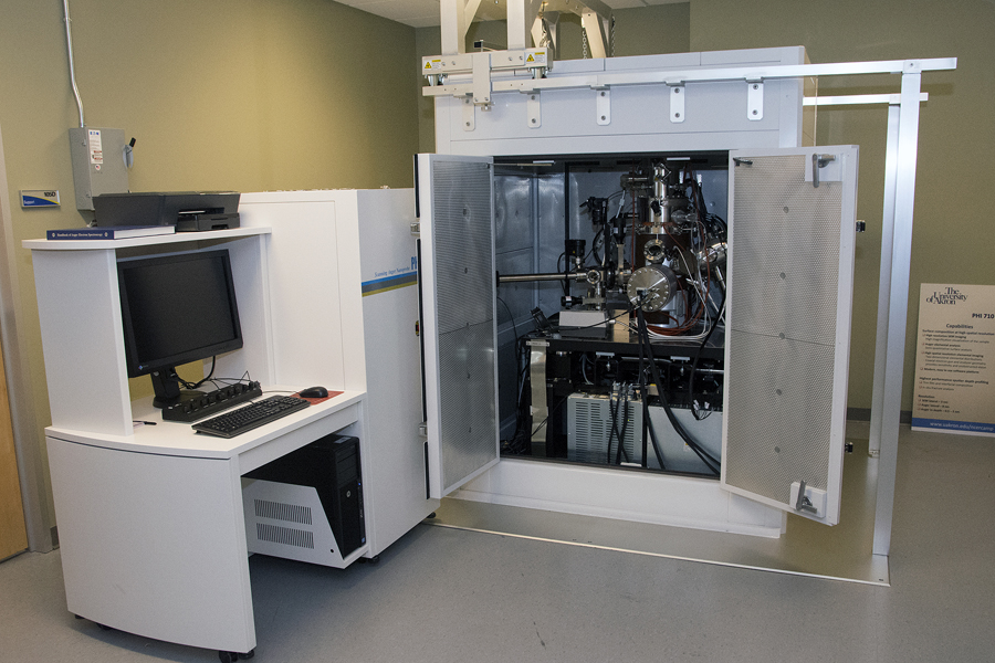
PHI 710 Scanning Auger Nanoprobe
Background
Auger Electron Spectroscopy (AES) is a technique that obtains specific elemental, so called Auger spectra from a depth of approximately 5 nm at a lateral resolution as small as 5-8 nm. Auger spectra are obtained in ultra-high vacuum after the sample is probed by a focused electron beam and are result of a multistep electron interaction process. Emitted Auger electrons have specific energies that are directly related to the energies of the inner electron shells of the elements. By measuring the kinetic energies and intensities of Auger peaks, the elemental identities and quantities of detected elements can be determined. Chemical state information is available from the measured peaks position and observed peak shapes. Depth distribution information (depth profiling) is obtained by combining AES measurements with ion milling (sputtering) to characterize thin film structures in the range of 10-100 nm.
The Phi 710 Scanning Auger Nanoprobe (SAN) integrates a high resolution SEM with a high resolution scanning Auger which provides a very important and unique capability: it can scan the probing electron beam across a predefined area with a spatial resolution of 8 nm and thus provide elemental maps on the nanoscale. These elemental maps or chemical images can be obtained for a selection of elements of interest and compared to the topographical SEM images obtained in the same instrument for the same region and having a resolution of 5 nm. Thus the Auger nanoprobe provides the most unique combination, not available on other instruments, of nanoscale SEM imaging combined with nanoscale elemental imaging.
Nano- and micro- scale regions on the samples can be studied easily and fast using these advanced capabilities. The instrument design using a coaxial electron gun and analyzer geometry provides the sensitivity and unobstructed vision needed to fully characterize and image the nano- and micro- structures that exist on real world samples with AES. Auger data is obtained from all sides of domains/particulates and between domains/particles with equally high sensitivity.
Applications
Conductive, semiconductor, ceramic samples, metals, alloys, lubricants; corrosion; thin film and interfacial composition research; defect and particle analysis in material performance research; failure analysis; tribology research; medical devices research; cutting and drilling tools surface quality control; information on the bonding state of metals and alloys; analysis of interface boundaries (alloys and coatings), lateral composition uniformity in thin films; metallurgical research, thin film devices for photonics and energy conversion
Specifications
- Multi-techniques Ultra High Vacuum (UHV) test chamber with ports able to accommodate Focused Ion Beam (FIB), Energy Dispersive Spectroscopy (EDS), and Electron Back Scattered Diffraction (EBSD) attachments
- Precision cylindrical mirror analyzer for minimum shadowing and maximum sensitivity
- Schottky field emission electron gun with high spatial (5 nm) resolution and large energy range (1-25 keV)
- High sensitivity, high contrast scintillation detector for secondary electron imaging
- Fully motorized, computer-driven five-axis precision specimen stage for rapid, accurate and easy positioning
- Full analytical capability including secondary electron imaging, multiple locations Auger points, linear and area analysis, Auger imaging, depth composition analysis, and automated multi-sample or multi-location analyses
- Auger spectral window mapping with spectra acquired at each pixel with user selectable high energy resolution for chemical state imaging
- 60 mm specimen introduction and magnetically coupled transfer system with a magnetically levitated turbomolecular pump and automated valve controls for rapid sample handling
- Fully software-controlled system that allows for remote internet operation
- 5 kV floating column argon ion gun for surface cleaning, charge neutralization, and Auger compositional depth profiling after sputtering at high or low impact energies